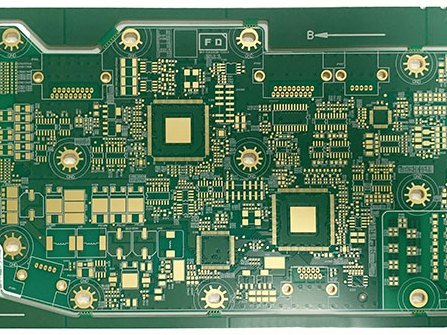
Density is now a packaging decision before it is an electrical one. A 0.4 mm pitch BGA does not merely ask for finer lines and tighter registration. It asks the board to carry escape routing, deliver power through the package, and move the resulting heat away — while the mechanical envelope around it shrinks at the same time. The board, the enclosure and the assembly process have to be designed as one object, because each one constrains the other two.
Electrically, density pushes the layer count up. Escape traces from a fine-pitch array need layers that are not doing anything else, so a six-layer stack may already be a compromise rather than a specification. Physically, that means a thicker board: lower Z-axis expansion tolerance, less thermal conductivity in the Z direction, and a stiffer response to reflow. Microvia stacks help by putting the interconnect close to the die, but they also concentrate heat in the region where the heat already is.
Thermally, the design has to decide where the heat goes. Through-hole thermal vias under the package, a copper pour on the opposite side, and a laminate with adequate thermal performance are no longer optional details for power-hungry parts — they are part of the electrical design. The thermal path continues through the interface material and into the enclosure, so a board that works thermally on the bench can still fail inside a sealed housing with no convection path.
Mechanically, smaller features mean larger keep-outs. Pick-and-place nozzle access, AOI and X-ray visibility, and the space a technician needs for rework all grow as the pitch shrinks, and they grow into a board that no longer has room for them. Warpage tolerance becomes critical as the board gets thinner and larger in area, because a bowed board will not seat into a connector or accept a BGA solder joint consistently. These effects show up at the customer, not in the fab, which is why they have to be designed in rather than discovered in the field.