
Inquiry
Send Gerbers, a stack-up or even a sketch. The scope of the build is confirmed in writing before anything is priced.
Indicative ranges for seven product families — rigid and flex boards, rigid-flex combinations, laser-microvia HDI, metal-core and heavy-copper power boards, and tested assemblies. Every figure published here is checked against your drawing before a panel is cut.

Chongshuo Electronics Technology Co., Limited (深圳市重硕电子科技有限公司) manufactures bare boards and finished assemblies in Shenzhen, China. A structure is chosen against the mechanical, thermal and electrical requirements of the product rather than against a catalogue, and the stack-up, copper weight, surface finish and hole sizes are fixed in writing before the first panel is cut. The ranges below are typical working values, not guarantees.
Every range, dimension and tolerance published on this page is indicative and typical, and is not a guarantee. Each figure is confirmed against your drawing, stack-up and manufacturing data package during DFM review and quotation, and the achievable value may vary with laminate type, board thickness, copper weight, surface finish and feature density. The values confirmed in writing in your quotation and order acknowledgement are the ones that govern production.
Each family, the construction behind it, and the typical layer range we work to. The parameters that sit behind these figures are set out in the sections below.
| Product | Structure | Typical Layer Range | Typical Application |
|---|---|---|---|
| Rigid PCB | Rigid FR-4, single, double or multilayer stack | 1–32 layers | Control equipment, power supplies, industrial and consumer electronics |
| Flexible PCB | Polyimide flex, static or dynamic | 1–8 layers | Camera modules, wearables, sensors, thin internal harnesses |
| Rigid-Flex PCB | Rigid and flex zones in one board | 2–16 layers (rigid and flex combined) | Wearables, camera modules, battery packs, robotics joints |
| HDI PCB | Sequential lamination with laser microvias | 4–20 layers | Fine-pitch BGA, mobile devices, miniaturised IoT products |
| Metal-Core PCB | Aluminium or copper base core | 1–4 layers | LED lighting and drivers, power modules, inverters |
| Heavy Copper PCB | Plated heavy copper, low layer count | 1–8 layers | EV charging, inverters, power conversion, industrial drives |
| PCB Assembly | SMT and through-hole, built and tested | SMT + THT (board layers per drawing) | Finished assemblies, box builds, functional-tested units |
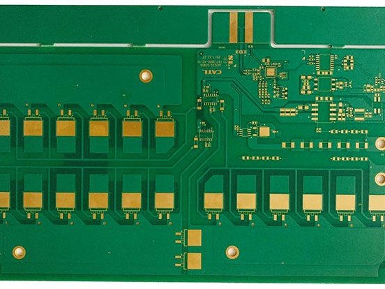
Rigid boards account for most of the work on the floor. A single-sided control panel and a 32-layer backplane are built in the same family, but they are not the same job — the stack-up, the impedance rules and the copper balance are engineered separately for each. Laminates run from FR-4 through high-Tg and halogen-free grades, and the surface finish is picked from the soldering process rather than from habit. Copper weight, board thickness and hole sizes are settled in writing before the first panel is cut, so the board you approve is the board that ships.
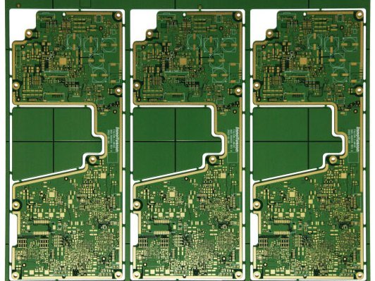
A flexible circuit is a different mechanical discipline, not a thinner rigid board. Where the circuit flexes repeatedly it is built on polyimide film with rolled copper; where the bend happens once during assembly, a stiffer static-flex construction is used instead. Bend radius, neutral-axis placement and copper weight are reviewed against the folding cycle stated in your drawing. Coverlay, stiffeners and shielding are specified alongside the copper, because those three decide how the finished flex behaves inside its housing.
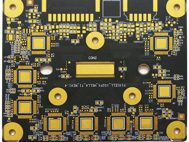
One part with two behaviours: a rigid-flex board carries the stiffness of a rigid section and the routing freedom of a flex section at the same time. The transition between them — bonded, laser-cut or bookbinder — is where most design problems appear. Bend radii, layer transitions, copper-to-flex termination and the position of components are reviewed before the stack-up is fixed. Where a flex section has to carry a controlled impedance, the flex layers are built to the same rule as the rigid layers and verified on coupon.
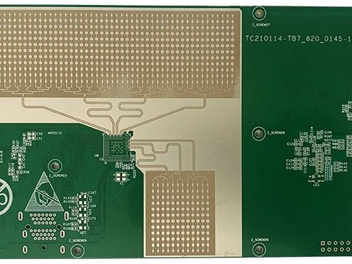
HDI is a sequential build rather than a simply thinner board. Each lamination cycle adds wiring density that a conventionally drilled stack cannot reach, and every cycle is another point at which the design can drift. 1+N+1, 2+N+2 and maked-up any-layer structures are built with laser microvias, filled and copper-capped where the drawing calls for it. Core artwork is prepared at the finished line width instead of being scaled afterwards, so fine-pitch land patterns stay manufacturable.
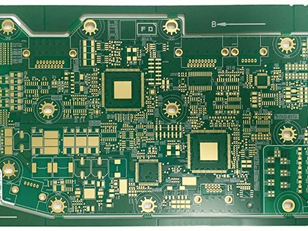
Swapping the FR-4 core for aluminium or copper is what a metal-core board is for: heat. The core carries heat sideways across the panel instead of letting it collect in one spot, which is what keeps an LED junction or a power switch inside its temperature limit. Core alloy, thickness and the isolation prepreg are selected from the mechanical and electrical requirements in the drawing, including any creepage and clearance distance the isolation layer has to hold. Finish selection matters here as well — carbon ink or matte black is used on LED boards for appearance, while the conductive pads still need a solderable finish.
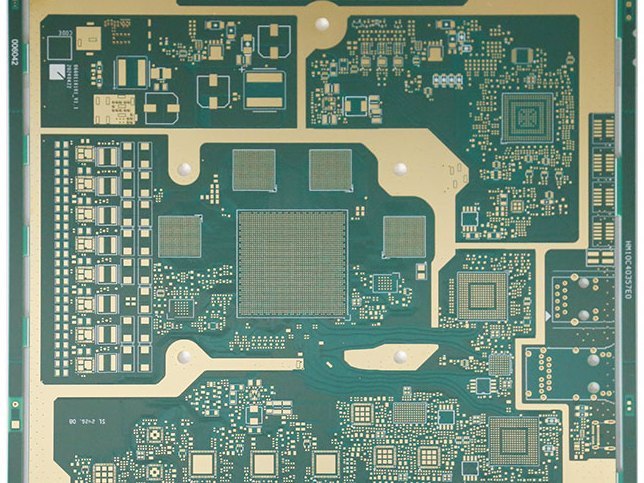
Heavy copper answers a question about current: a conductor that has to carry more than a standard copper layer can. The copper is built up by plating rather than laminated as thick foil, which keeps the layer count low and means the artwork has to be compensated for the extra etch depth. Copper and laminate in the same stack expand at different rates, so the build is reviewed for thermal cycling rather than assumed to survive it. Plating thickness, hole size and minimum trace width all move together on this kind of board.
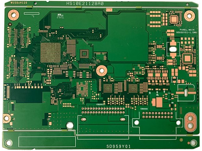
Assembly is where a board either works or does not, and it is where most of the risk in an order sits. Components are sourced against your approved vendor list, and every substitution is put to you in writing before it is used, because a different part number on the same footprint is not the same part. SMT and through-hole work are combined on the same board where the design needs both, including BGA and QFN packages. Programming, inspection and functional test are part of the build rather than an offer afterwards, and the unit can be boxed, labelled and packed to your instruction.
A unit is complete only when the fitted components are the ones you approved, the firmware has been programmed and the functional test has passed. The assembly BOM and the test results are delivered with the shipment instead of staying in the shop.
Eight checkpoints between your files and your receiving dock. You always know which one the order is at, and what it is waiting for.
Send Gerbers, a stack-up or even a sketch. The scope of the build is confirmed in writing before anything is priced.
Your files are checked against the process that will actually run them, and the findings come back as specific points.
Itemised pricing by layer count, material, copper weight, surface finish and quantity, so each driver sits on its own line.
Stack-up, impedance rules, drill and routing data are prepared and agreed with you before production is released.
Laminate, imaging, etching, drilling, plating, solder mask and surface finish, to the approved specification.
AOI and electrical test on every board, plus dimensional checks against the drawing.
Optional SMT and through-hole assembly, firmware programming and functional test on the same purchase order.
Packed with the documentation that describes it, and shipped door to door on EXW, FOB or DDP terms.
Gerbers, a stack-up, or just the question you are stuck on. We answer inquiries during Monday to Saturday, 9:00–18:30 (GMT+8).